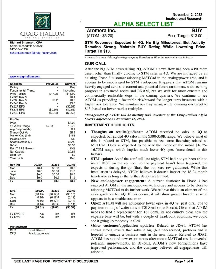
Craig Hallum report takes no credit for Memory or Advanced Nodes and those will be highest royalty generators with high volume and huge wafer prices. Very high TAMs.Works Across All Nodes
Follow me on Twitter @microcapreturns
Https://GainTherapeutics.wordpress.com
Https://atomerastockreport.wordpress.com/
These reports are generated by the author and not affiliated with any of the companies discussed.
Any due diligence from this site is for entertainment only and not a solicitation to buy or sell Atomera stock. Any estimates are just examples of what is possible and should not be considered financial advise. I have not been compensated in any way and will never be compensated for my reports.
Craig Hallum Moonshot Potential from 2021 early coverage and before RF-SOI, GAA and DRAMCraig Hallum report takes no credit for Memory or Advanced Nodes and those will be highest royalty generators with high volume and huge wafer prices. Very high TAMs.
Follow me on Twitter @microcapreturns
Https://GainTherapeutics.wordpress.com
Https://atomerastockreport.wordpress.com/
These reports are generated by the author and not affiliated with any of the companies discussed.
Any due diligence from this site is for entertainment only and not a solicitation to buy or sell Atomera stock. Any estimates are just examples of what is possible and should not be considered financial advise. I have not been compensated in any way and will never be compensated for my reports.
Quarter 2 webcast/transcript and new full investor presentation
LD Micro October Presentation
Craig Hallum Moonshot Potential from early coverage and before RF-SOI, GAA and DRAMCraig Hallum report takes no credit for Memory or Advanced Nodes and those will be highest royalty generators with high volume and huge wafer prices. Very high TAMs.
Follow me on Twitter @microcapreturns
Https://GainTherapeutics.wordpress.com
Https://processastockreports.wordpress.com
Https://atomerastockreport.wordpress.com/
Joesstockreports: Absolutely free information on stocks I own
These reports are generated by the author and not affiliated with any of the companies discussed.
Any due diligence from this site is for entertainment only and not a solicitation to buy or sell Atomera stock. Any estimates are just examples of what is possible and should not be considered financial advise. I have not been compensated in any way and will never be compensated for my reports.
These reports are generated by the author and not affiliated with any of the companies discussed.
Original Craig Hallum NoteSamsung Gate All Around Patent references AtomeraSamsung Patent has 5 Atomera references Craig Hallum report takes no credit for Advanced Nodes even those will be highest royalty generators with high volume and huge wafer prices.Company has stated current customers are Leading Semiconductor Companies and follow example 2Advanced Nodes Under 5nm are crazy royalties
Any due diligence from this site is for entertainment only and not a solicitation to buy or sell Atomera stock. Any estimates are just examples of what is possible and should not be considered financial advise. I have not been compensated in any way and will never be compensated for my reports.
This agreement enables ST to install Atomera’s Mears Silicon Technology™ (MST®) into its facilities and authorizes ST to manufacture and distribute MST-enabled products to its customers.
Upon completion of wafer-level qualification, ST will officially begin production, which will trigger another milestone payment and grant them the right to manufacture and sell product incorporating Atomera’s technology.
Joe’s Q1Summary: The biggest news was the signing of the STMicro commercial license. Why is this significant? This license has already negotiated the Phase 4(tech transfer), Phase 5(manufacturing license) and the Phase 6(production royalties on manufacturing). This is the first customer who has committed to production parts and wouldn’t do the install unless they were going into production. No reason to invest the tech transfer money and modify a $30m Applied Materials EPI tool. The difference between this deal and JDA 1 is the JDA 1 customer has approved it for usage in all their fabs and now Atomera works with each business unit to get them to adopt. Each will need to commit to a manufacturing license and royalty schedule. That has already been negotiated with STMicro. Now its just complete the milestones to get into production. The biggest difference between JDAs and STMicro deal is upon completing tech transfer and wafer verification STMicro goes right into production. When that is we wait to see but it could mean production royalties much sooner than explained on call. While STMicro may have the clearest path to royalty generating production I still think JDA 2 may be first. See comments below.
Likewise, work with JDA #2 is ongoing with new experiments to follow up on our initial trials and as specified in our JDA, if we can meet thoserequirements, we will have milestone payments to announce. We are also active with each of our 4 other licensees, including ST, we’ve discussed earlier, and AKM, who had gone into a pause after a fab fire in 2020. We are now planning to resume our work with AKM either at their facilities or through a foundry partner.
Q1 Summary(cont): While updates on the pipeline customers were overshadowed by the STMicro license there was a comment about JDA 2. JDA 2 which was announced about a year ago looks like if they get results they expect will move forward with what I think will be some type of Phase 4 tech transfer milestone. The significance is since this JDA always was trying to solve problems it might be used for something such as doping which means it could go into production much quicker than STMicro. This is a key item to watch for.
Second Phase 4 to be added as STMicro installs MSTAmazing 38% improvement adopting MST into this segment
Q1 Summary(cont): The announcement of MST-SPX is significant for multiple reasons. The first being even small improvements in performance in this space are significant and are worth adopting. Companies have been squeezing out every percentage of performance in this sector for years and the biggest concern for them when adopting a new technology is reliability. This move signals they must have data not only showing performance improvements but no impact on reliability. An excellent place to be is where customers need solutions and Atomera can provide large improvements in performance. MST-SPX is also important for this market since these are premium parts and will carry nice royalties for markets like EVs. They will pay the premium for more performance.
Q1 Summary(cont): The company sold under 50k shares using the ATM for the first quarter. They did not believe the share price was representative of its value. The company continues to wisely use the ATM and minimize dilution. Payments from future milestones will further reduce cash usage going forward.
Q1 Summary(cont): A question at the very end on 3/2nm node royalties is significant. These are the new nodes for TSMC, Intel and Samsung also known as the Big 3. They are the only ones developing fabs like this although IBM does have 2nm process they are developing to license to third parties. Scotts answer indicated Atomera understands the extremely high royalty rate that an advanced node generates with wafers around $20k each and potential volume over 100k wafers per month. The company has already had some discussions with potential licensees in this area and hope more info soon. I expect this to be a large upfront payment and smaller royalties. Plenty of cash for Atomera and recurring numbers that fabs will pay. This will speed adoption into next generation fabs. One deal in this area will create a runway where they never will raise money again and cash can be used to maximize shareholder benefits.
Q1 Summary(cont): Craig Hallum raised price target to $17. They still have not factored in any next generation fabs which will likely be structured more like a biotech deal and weighted with a heavy upfront and reasonable royalties on expensive wafer/parts fabs. See below for note.
Foundational plus device design patents enabled by MSTLow cash burn and minimal dilution makes this investment unique
CompanyCC Highlights
$17m in cashand 23.66m shares o/s end of Q1 2023 compared to 22.85m end of Q1 2022.
Used $4m in cash and sold 50k shares in Q1 2023
4.5m shares short as of 4/13/23
Used ATM in Q1 selling 50K shares in Q1. In the last year used $7m in cash and shares outstanding increased by 800k shares. Low cash burn and minimal share dilution.
I’d like to take a moment and highlight one new area of development we have underway that shows very strong potential. In discussions with customers about our 5-volt power management focused solutions, we are consistently asked if MST can help for higher voltage transistors up to the 40-volt range used in a wide set of applications requiring greater power. Over a year ago, Atomera started designing silicon to enhance these very hard to improve devices. Our early test data shows very promising results, and this slide gives one of the most important specs from our first silicon.
As discussed in the past, we continue to believe that development of these incredibly difficult and costly next-generation nodes will require an industry-wide cooperative approach that Atomera has become part of, and we believe these efforts will yield fruit through license activity in the future.
Atomera joins American Semiconductor Innovation Coalition (ASIC) | Atomera
As you may have seen in recent semiconductor earnings announcements that are now — that now — that we now appear to be at the bottom of the semiconductor cycle. How long we stay here, it’s an open question, but we continue to see this year as a prime period to engage with customers to add MST to their manufacturing technology tool bag. So our focus has to be on acquiring new customers and getting existing ones over the hump and into the licensing phase while the timing is right.
But I do think in the more advanced nodes, we would be able to get a higher royalty rate, in terms of dollars per wafer, and they run in very high volumes. But we would have to be realistic about charging or wafer price that they find palatable. So haven’t negotiated one of those yet, have had some discussions, and I hope that’s something that we have to worry about soon.
JDA#1 Customer – Leading Semiconductor Company1/5/21
Meets Requirements of JDA Agreement 4/14/22 which opens door to business units and applications area
World Class Fabin South Korea
High Capacity
We also hit a significant milestone in our JDA partnership with a large semiconductor manufacturer.
Successful outcome to this JDA was necessary so we can start moving those business units forward on MST integration and toward commercial royalty-bearing production
Our customer is satisfied that Atomera’s technology meets their challenging requirements, which validates the manufacturability and the effectiveness of using MST in a world-class fab.
But the important thing is our technology has been proven to do what we said it would do.
We believe the advancements in our JDA program will spur competitive pressures on all of those in our pipeline to move faster
$300k payment was made as part of $700k JDA fee
“Atomera is thrilled to join with an industry leader that has a strong record of technology innovation to extend Moore’s Law,” said Scott Bibaud, president and CEO, Atomera.
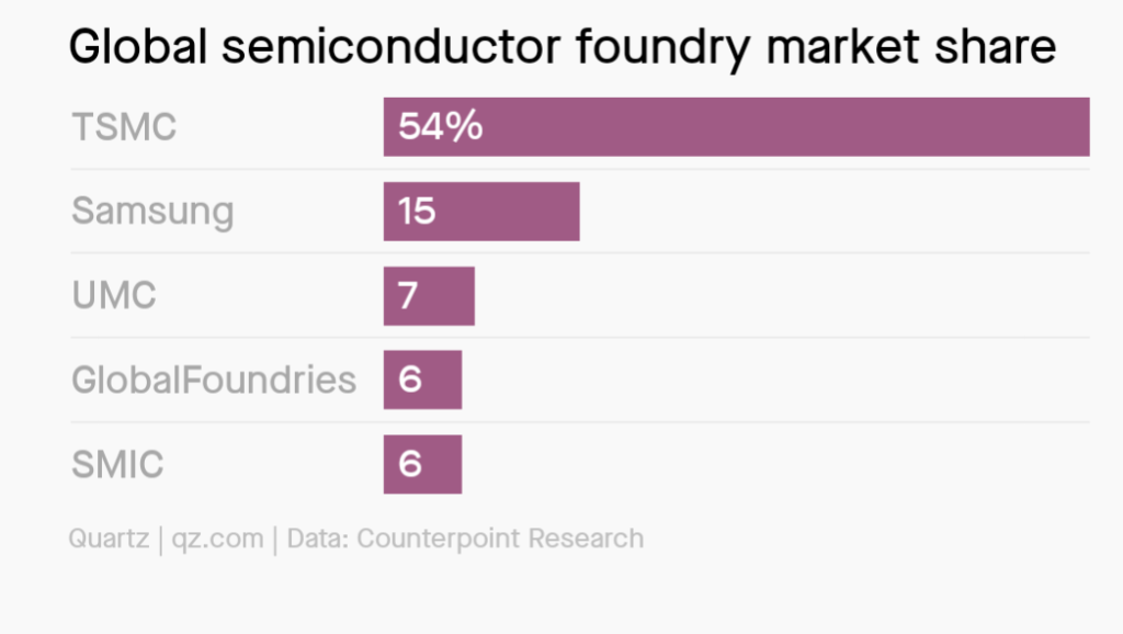
Largest Foundry Market Share
JDA #2 Customer – Major Semiconductor Foundry4/27/22
High Capacity
Atomera announced that we entered into our second JDA, this time with a large semiconductor foundry who’s been working with us in phase 3 for a number of quarters.
This new JDA we announced today is pretty focused around one specific business. And if all goes well, they’ll be driving that specific one to get into production, and hopefully, will get adopted by other business units inside their company.
The purpose of which is to define exactly what steps will be taken with high priority and with a full set of resources to take MST-based products into production, if the results of our latest experiments meet their expectations.
Now, the first milestone requires us to get good results on some work that we’re doing together right now. But, the whole point of the JDA is to kind of grease the skids, that if we get good results on that next one — and we’re very confident.
That said, if we’re successful on this JDA, we believe the customer will move expeditiously towards commercialization because the all the legal and contract delays should be behind us.
But we do have a number of other areas that we have been talking with them about and has the real potential to expand beyond, into those once we’ve established success in this first area.
Foundry License – World Class Foundry 2/8/22
High Capacity
$75k license paid in q1 from North America
Licensee that started in February, and obviously, we’re going very hot and heavy with them.
Foundry partner very well known in the industry for bringing innovative technologies to market.
We started our engagement with them some time ago, so they are already a Phase 3 customer
Over the last year, they have used our MSTcad modeling software to unveil some compelling new uses of MST that may enhance some of their specialty processes.
Once that advantage was made clear to them through our modeling software, they immediately took steps to start running MST on device wafers.
Electrical results, which validate the modeling run by this new licensee, would be a breakthrough in performance that I think they would be extremely enthusiastic about taking into production.
Obviously, if our technology is adopted by a foundry and made a standard process, it opens the door to fabless design companies around the world designing chips that can be used in our process, and that’s quite exciting to us.
Any due diligence from this site is for entertainment only and not a solicitation to buy or sell Atomera stock. Any estimates are just examples of what is possible and should not be considered financial advise. I have not been compensated in any way and will never be compensated for my reports.
These reports are generated by the author and not affiliated with any of the companies discussed.
Original Craig Hallum NoteCraig Hallum report takes no credit for Advanced Nodes even those will be highest royalty generators with high volume and huge wafer prices.Company has stated current customers are Leading Semiconductor Companies and follow example 2Advanced Nodes Under 5nm are crazy royalties
Any due diligence from this site is for entertainment only and not a solicitation to buy or sell Atomera stock. Any estimates are just examples of what is possible and should not be considered financial advise. I have not been compensated in any way and will never be compensated for my reports.
Joe’s Q4Summary: Travel activity is up over 400% since the same period last year. It involves both existing and new opportunities. The key with licensing is the most progress happens during face to face meetings which means this is significant sign that the industry has capacity to work R+D projects and is looking for solutions from legacy nodes to bleeding edge nodes. Also company is looking to hire to support all current and future opportunities. I expect business to explode once the first customer goes into Phase 5 as an industry wide validation of the technology.
Q4 Summary(cont): Last quarter the CEO discussed how some companies had completed all their required testing and were just waiting for the right time to go forward. This quarter there was discussion how large companies approve technology and it sits on the bench waiting to implement into production. This could be JDA 1 having completed testing and waiting to go forward depending on factory timing and products.
Q4 Summary(cont): The pipeline had the one Phase 2 move to Phase 3. All the JDA and Licenses continue making progress. For the first time on the chart the colors for Phase 5 and Phase 6 are shown.
Phase 5/6 shown on chart
Q4 Summary(cont): The company sold around 700k shares using the ATM for the year. Only 109k in November and none since then. They have over $21m is cash and burn around $3m/quarter. They have shown a very wise approach to using ATM and have shown no reason why that won’t continue and that they have no intention or need to sell shares at these levels.
Q4 Summary(cont): The company announced there will be a new version of MST-SPX coming in the future that will benefit the high voltage parts that dominate the Electric Vehicle market. These are premium priced parts that require the top performance for efficiency and reliability.
Q4 Summary(cont): Good discussion about their patent portfolio. As Scott mentionedthey have 339 issued and in progress and each of those have over 20+ claims giving them wide spread coverage and making it impossible for anyone to use the technology without licensing. The company not only is a material science company but recent patents make them a device designer company that knows how to best apply MST across all markets.
Foundational plus device design patents enabled by MST
CompanyCC Highlights
$21.2m in cashand 24m shares o/s end of 2022
Used $7.5m in cash and sold 700k shares in 2022
4.25m shares short as of 2/28/23
Used ATM in Q4 selling 109K shares in November and have not sold any shares since
Right now, we have no exposure to China. We have a lot of interest around the world and I think there’s too much uncertainty about how far we’ll be able to take our technology within China for us to make that — to move it up into the priority chain for us on our business development activities.
This part of the semiconductor economic cycle is where Atomera thrives. Due to fab overutilization, our customers have postponed their normal development efforts for the last few years. So, there’s now pent-up demand for improvements that must be executed, particularly in the application areas, which experienced the greatest constraints.
So, this chart on Slide 4, unfortunately, does not do a great job showing our progress. In searching for a metric that can illustrate our activity level better, I found that travel to customers for new projects is up between 450% to 500% over the last 3 months versus the same period last year. This rate of close customer engagement is not letting up and I am confident it will result in more licensing opportunities over the next few quarters.
We do expect to see a growing customer pipeline and to announce additional licensees in the months ahead.
During the last quarter, we have seen unprecedented interest and activity in the leading digital nodes where our technology provides a number of benefits for 3D technologies, as discussed on our last call and shown on this slide.
I am confident we’ll be able to make exciting customer announcements like that during the course of this year. In the meantime, morale inside Atomera is running very high. We are so busy with customer projects and new developments, we’re straining to keep up. There is no doubt that at this pace, we will need to add resources to handle all of our new opportunities. We continue to believe strongly in a future where licensing activity, followed by commercialization will make Atomera a recognized innovation leader in the semiconductor industry.
One of the things I’ve talked about in the past, but I’d like to really reiterate now is, a lot of times, you work with a big customer, you get results that look really good, but they don’t immediately move forward with it because they just aren’t funded to do an R&D path or make a new process technology come out that year. So, it sits on the bench. But at some point, they take it off the bench and they say, okay, now we’re ready to go. And so we — with what we’re seeing in the industry and the interest we’re seeing from new customers and existing customers, we’re hopeful that some of those things will come off the bench and we’ll start to see things moving towards production now.
JDA#1 Customer – Leading Semiconductor Company
World Class Fabin South Korea
High Capacity
We also hit a significant milestone in our JDA partnership with a large semiconductor manufacturer.
Successful outcome to this JDA was necessary so we can start moving those business units forward on MST integration and toward commercial royalty-bearing production
Our customer is satisfied that Atomera’s technology meets their challenging requirements, which validates the manufacturability and the effectiveness of using MST in a world-class fab.
But the important thing is our technology has been proven to do what we said it would do.
We believe the advancements in our JDA program will spur competitive pressures on all of those in our pipeline to move faster
$300k payment was made as part of $700k JDA fee
“Atomera is thrilled to join with an industry leader that has a strong record of technology innovation to extend Moore’s Law,” said Scott Bibaud, president and CEO, Atomera.
Largest Foundry Market Share
JDA #2 Customer – Major Semiconductor Foundry
High Capacity
Atomera announced that we entered into our second JDA, this time with a large semiconductor foundry who’s been working with us in phase 3 for a number of quarters.
This new JDA we announced today is pretty focused around one specific business. And if all goes well, they’ll be driving that specific one to get into production, and hopefully, will get adopted by other business units inside their company.
The purpose of which is to define exactly what steps will be taken with high priority and with a full set of resources to take MST-based products into production, if the results of our latest experiments meet their expectations.
Now, the first milestone requires us to get good results on some work that we’re doing together right now. But, the whole point of the JDA is to kind of grease the skids, that if we get good results on that next one — and we’re very confident.
That said, if we’re successful on this JDA, we believe the customer will move expeditiously towards commercialization because the all the legal and contract delays should be behind us.
But we do have a number of other areas that we have been talking with them about and has the real potential to expand beyond, into those once we’ve established success in this first area.
Foundry License – World Class Foundry
High Capacity
$75k license paid in q1 from North America
Licensee that started in February, and obviously, we’re going very hot and heavy with them.
Foundry partner very well known in the industry for bringing innovative technologies to market.
We started our engagement with them some time ago, so they are already a Phase 3 customer
Over the last year, they have used our MSTcad modeling software to unveil some compelling new uses of MST that may enhance some of their specialty processes.
Once that advantage was made clear to them through our modeling software, they immediately took steps to start running MST on device wafers.
Electrical results, which validate the modeling run by this new licensee, would be a breakthrough in performance that I think they would be extremely enthusiastic about taking into production.
Obviously, if our technology is adopted by a foundry and made a standard process, it opens the door to fabless design companies around the world designing chips that can be used in our process, and that’s quite exciting to us.
CH Update
Any due diligence from this site is for entertainment only and not a solicitation to buy or sell Atomera stock. Any estimates are just examples of what is possible and should not be considered financial advise. I have not been compensated in any way and will never be compensated for my reports.
Longer DRAM refresh interval: DRAM bitcells must be refreshed when the charge onthe (worst) capacitor leaks sufficiently that a ‘1’ cannot reliably be read. Refresh consumes significant power – some studies show it consumes 30% of the total DRAM power budget, and 10-13% of total server power. A better sense margin enables a longer interval between refreshes, reducing power proportionally, possibly by 50% or more!
DRAM WHITEPAPER
In-person presentation of San Jose State’s and Atomera’s joint poster, entitled “Cryogenic Electron Mobility and Subthreshold Slope of Oxygen-Inserted (OI) Si Channel nMOSFETs”
Professor Hiu Yung Wong of San Jose University, Robert J. Mears, CTO, and Hideki Takeuchi, Vice President of Engineering of Atomera Incorporated (Nasdaq: ATOM)
Wednesday, September 27 from 11 p.m. – Thursday, September 28 12:30 a.m. PDT, Thursday, September 28 from 3 p.m. – 4:30 p.m. JST
This poster presentation will discuss the new findings of the physical mechanism of why MST®
Atomera’s MST film improves surface-roughness scattering by 53% compared to a regular Si channel
MST improves Coulomb scattering, which is significant at low vertical effective field, by reducing ionized dopant impurities near the gate dielectric
A simple analytical formula to describe the observed mobility behaviors of the MST film has been established for compact modeling.
SISPAD Poster
Atomera Incorporated – Events & Presentations
Atomera Second Quarter Fiscal Year 2023 Financial Results Conference Call and Video Webcast August 2nd, 2023
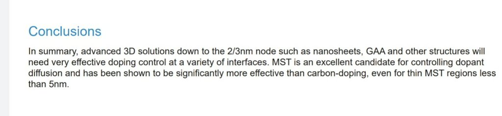
One of the biggest challenges in semiconductors is to keep lowering power consumption as the nodes get smaller. A phenomenon that prevents them from doing so is something called random dopant fluctuation or RDF, which are variations in concentration of the implanted dopants, and the impact of those variations becomes more significant as the nodes size get smaller.
The good news is that MST is very adept at mitigating the problem of RDF. Our analysis shows that in the latest gate-all-around transistors, a single dopant atom diffusing into the channel can significantly alter the transistor’s characteristics. This is why the dopant control characteristics of MST are so important for advanced node customers.
So our analysis shows and gate all around transistors, which are — as you know, they’re going to be adopted by the foundries at very small process nodes, probably in the 3 and 2-nanometer level.
But in this case, the channel is so small that 1 or 2 Atoms moving into the channel increases the concentration of dopants in that channel significantly. And they want the channel to be as clear of dopants as they can possibly make it.
So by implementing MST, which really improves the chances that they won’t see random dopants going into the channel, we can bring a big improvement in reliability from that perspective and performance.
Atomera joins American Semiconductor Innovation Coalition (ASIC)
Jeff Lewis, SVP Business Devt. and Marketing April 12th, 2023
Bringing to market the next generation of microelectronics technology is too complicated for one company to do on its own, requiring an innovation ecosystem of the most talented companies and resources.
As MST® can provide benefits across the industry from the most advanced gate-all-around (GAA) nodes to DRAM and legacy analog and power nodes, we are participating in the following ASIC workstreams
By Brian Bailey with quotes from Robert Mears(CTO Atomera), Julien Ryckaert, vice president of R&D at imec, Victor Moroz, fellow in the TCAD product group of Synopsys.
Why are we making this change? “If finFET pitch could continue scaling, people would have stayed with finFET,” says Julien Ryckaert, vice president of R&D at imec. “The problem is finFET cannot scale simply because you need to plug the gates, work function stack, in between two fins.
The device benefit is that MST devices can have a lower threshold voltage for the same grown hafnium oxide thickness.
Intermixing reduction in ultra-thin titanium nitride/hafnium oxide film stacks grown on oxygen-inserted silicon and associated reduction of the interface charge dipole
This discovery opens up a new technique for tuning HKMG electrical characteristics.
OI-Si promises significant performance boost for the end-of-roadmap planar CMOS products with HKMG stack due to its unique carrier mobility improvement,34 gate leakage reduction,34 and reduction of random dopant fluctuations.35 In addition, the newly observed interfacial charge dipole reduction opens an opportunity for OI-Si as the metal work function tuning layer in HKMG-based semiconductor products, which is particularly important for next generation non-planar CMOS.
HKMG Devices Work Better With MST, Extending the CMOS Roadmap
Announcing Atomera’s Latest White Paper: “MSTcad for PMIC and RF-SOI Switches”
Authored by Atomera’s founder and CTO, Robert Mears and VP Engineering, Hideki Takeuchi, this document provides an overview of MST and its benefits, and describes how to model MST using MSTcad, as well as, demonstrates the significant benefits of using MST to improve PMICs or other power devices and RF-SOI switches.
Using wafers from Soitec, Atomera has been able to demonstrate the unique dopant retention of MST on ultra-thinned RF-SOI substrates.
MST enables greater than a 10x steeper SSRW profile by implanting boron into the SOI substrate after blanket MST epi growth.
MST® for PMIC and RF-SOI Switches
News Blog Post from Atomera Incorporated
Announcing Atomera’s Latest White Paper Demonstrating MST Advantages for the Most Advanced Semiconductor Processes
MST Advantages for the Most Advanced Semiconductor Processes
But in addition, we can now project that MST, in conjunction with HKMG, can also bring >15% higher mobility for GAA and hence higher performance metrics.
We expect to be able to engineer more than a typical node’s improvement in performance for a fraction of the development cost!
Smoothing the Surface: MST® Turbo-Charges GAA Devices
News Blog Post from Atomera Incorporated
White Paper: MST® Benefits for Gate-All-Around (GAA)
In this White Paper we outline some recent learning about Atomera’s MST® technology and how it can be used to improve advanced 3D devices, particularly gate-all-around (GAA) nanosheet devices (sometimes also called “RibbonFETs” or “Multi-Bridge Channel” (MBC) FETs).
1/4/23
The key MST benefits for these devices are dopant diffusion control [1], improved mobility[2,3], the recently discovered work-function engineering potential of MST [4] and MST’s ability to improve contacts by reducing the Schottky-barrier height [5].
Summary: This White Paper will show that MST can improve GAA devices in 4 ways:
Source Engineering on Oxygen-Inserted Si Channel for Gate Length Scaling of Low-Voltage Switch Devices
These results were demonstrated on silicon fabricated at an automotive-qualified foundry by shrinking the gate length of a baseline 5V analog MOSFET down to 0.25um, leading to a 100% increase in drive current compared to baseline devices.
Atomera to Present Keynote Speech at IEEE IMFEDK 2022 Conference
Atomera’s paper, entitled “Remote control of doping profile, silicon interface, and gate dielectric reliability via oxygen insertion into silicon channel.”
Wednesday, November 30 at 4:40-5:20 p.m. JST
Hideki Takeuchi, Robert J. Mears, Marek Hytha, Daniel Connelly, Paul E. Nicollian(Pres. Semi Rel Corp) and Hiu-Yung Wong(San Jose St)
Atomera’s paper will dive into the significant impact for HKMG stack as the MST layers reduce intermixing and interfacial charge dipoles, which lowers remote charge scattering and provides viable knobs for the performance boost and new designs of future electronic devices.
Although the opportunity in legacy nodes is quite exciting for Atomera, MST technology is also very well positioned to solve problems for customers at the leading edge.
Adoption in older fabs or newer 28nm fabs
Assume 2% royalties
Wafer royalty $66/wafer
IDM piece part royalty example .09/part
Using 80K wafers/month
Wafers $64m/node
IDM $255m/node
Adoption in next generation 5/3/2nm fabs
Assume 2% royalties
Wafer royalty
5nm $340/wafer
3nm $500/wafer
Range 20k-80k wafers/month
5nm wafers $81m – $326m/node
3nm wafers $125m- $500m/node
IDM Royalties typically 4X wafer royalties per node
Follow me on Twitter @microcapreturns
Https://GainTherapeutics.wordpress.com
Https://processastockreports.wordpress.com
Https://atomerastockreport.wordpress.com/
Joesstockreports: Absolutely free information on stocks I own
These reports are generated by the author and not affiliated with any of the companies discussed.
Any due diligence from this site is for entertainment only and not a solicitation to buy or sell Atomera stock. Any estimates are just examples of what is possible and should not be considered financial advise. I have not been compensated in any way and will never be compensated for my reports.
This Synopsys Seminar was given by Atomera’s Founder Robert Mears in March of 2022. These are screen shots of some of the presentation. Synopsys has restricted viewers to industry representatives so they know who to sell their TCAD software to. Here is the info.
These reports are generated by the author and not affiliated with any of the companies discussed.
Any due diligence from this site is for entertainment only and not a solicitation to buy or sell Atomera stock. Any estimates are just examples of what is possible and should not be considered financial advise. I have not been compensated in any way and will never be compensated for my reports.
These reports are generated by the author and not affiliated with any of the companies discussed.
Craig Hallum report points out huge earnings leverage and companies optimism that next stage events will happen soon. Report takes no credit for all the Advanced Node work even though just one advanced node can generate hundreds of millions in royalties for Atomera. His model continues to be outdated as the company has repeatedly said they are working with high capacity customers first that follow the 300mm 28nm examples as outlined on their slides. One of those 28nm nodes will provide over $60m/year in royalties and dwarf their moonshot case. Cash on hand is good for 6 quarters and they still have $45m left on ATM. That would take them out almost 5 years but company has shown very smart usage and dilution has been minimal with still under 24m shares outstanding.
Craig Hallum report takes no credit for Advanced Nodes even those will be highest royalty generators with high volume and huge wafer prices.Company has stated current customers are Leading Semiconductor Companies and follow example 2Advanced Nodes Under 5nm are crazy royalties
Any due diligence from this site is for entertainment only and not a solicitation to buy or sell Atomera stock. Any estimates are just examples of what is possible and should not be considered financial advise. I have not been compensated in any way and will never be compensated for my reports.