These reports are generated by the author and not affiliated with any of the companies discussed.
Any due diligence from this site is for entertainment only and not a solicitation to buy or sell Atomera stock. Any estimates are just examples of what is possible and should not be considered financial advise. I have not been compensated in any way and will never be compensated for my reports.
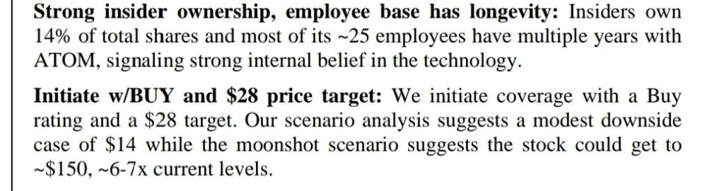
This Company slide shows how 1 fab can generate $63m by itself. Therefore if using company provided data 7 fabs would take this well over the Moonshot target. Original Craig Hallum Note
STMicro new Italy Plant goes to Phase 4 Tech Transfer
Foundry License goes to Phase 4
JDA 2 goes to Phase 4
JDA 1 goes to Phase 5 with multiple business units
Pipeline increases
Atomera to Announce Third Quarter 2022 Financial Results and Host Webinar on Wednesday, November 9, 2022
The company will host a live video Zoom webinar at 2:00 p.m. Pacific Time (5:00 p.m. Eastern Time) on Wednesday, Nov. 9, 2022, to discuss the results. The live webinar can be accessed through Atomera’s investor relations website at https://ir.atomera.com. A replay of the webcast will be available for 12 months.
Atomera Presented atOppenheimer 25th Annual Technology, Internet & Communications Conference
Aug. 9, 2022, with a presentation at 2:05 pm ET
HIGHLIGHTS
Atomera is working with the much larger fabs, big companies whose fabs are high capacity. One of our customer(see royalty slide example below) 28nm, who we would love to get into production.
Seeing preliminary results on wafer runs that make us very optimistic that we will be making progress in near future. Early peaks look very hopeful and hope to announce new licenses as result of wafer runs. Say a lot more in second half on results.
For GAA 3/2nm fabs can increase mobility by greater than 15% and have multiple uses for MST.
Financial perspective. Lean. Well capitalized, no debt and can get to the point of generating revenue in near future.
Once in Phase 4 Scott believes they will go into production given investment made by fab in terms of license, material and resources already spent to get to Phase 4.
No Brainer for Foundry and Fabless customers to adopt.
Company has always focused resources on Leading/Large Semiconductor Companies that are high Capacity/Royalties
But in addition, we can now project that MST, in conjunction with HKMG, can also bring >15% higher mobility for GAA and hence higher performance metrics.
We expect to be able to engineer more than a typical node’s improvement in performance for a fraction of the development cost!
Breakthrough will benefit 3/2nm fabs. Majority of customers are 300mm wafers where higher royalties will be paid.
Q2 Summary: The company added a new customer to its pipeline and all other licenses and JDAs are continuing to make progress with wafer runs. Preliminary data looks very promising and should expect to see movement in further Phase 4s and Phase 5 announcements this year.
Q2 Summary(cont): The biggest news in this quarters release was the release of the new whitepaper(see above). These are ground breaking results that are directly applicable to the next generation 3/2nm fabs that cost around $20b to build. The data shows that by utilizing MST these new fabs can improve performance by another full node i.e. a 3nm node get 2nm performance without any significant investment. The paper goes into great detail of why this is and my guess is the big three(TSMC, Samsung and Intel) will be verifying these results in the very near future. I have always said Atomeras MST technology is an enabler to benefit companies in areas of price or performance but these results make Atomera more of a disruptor. By this I mean adopting this technology could allow companies to leapfrog performance of competitors without spending tens of billions on a new fab. This is very significant for any next generation fab.
Q2 Summary(cont): The new chips act was discussed. The companies technology is well suited to help improve legacy nodes performance and that is where the company will look to provide value. If nothing else I think they will be able to get tax credits on all of their R+ D work going forward.
Increasing Pipeline with 6 customers with multiple engagements
CC Highlights
$21.8m in cash. Burn rate $3.5m/qtr
23.5m share o/s. Zero debt, no warrants
Used ATM in July selling 235K shares and raising $2.6m which will cover majority of Q3s cash usage.
Pipeline increased to 20 customers and 26 engagements
The second quarter was where new customer interest in projects with existing customers have really started to grow again.
Programs with all our licensees and JDA partners continues to make good progress
We have been able to look at some data prior to lot completion and have been very encouraged by the promising interim test results.
And in many cases, the actual results are exceeding both our expectations and those of our customers.
Now I’d like to take a few minutes to explain a quite important new discovery of made on MST for advanced nodes.
To our surprise and delight, it showed that MST enhanced electron mobility related to surface roughness scattering by over 50% which is a massive improvement and something particularly important in the advanced notes.
And this will be used to start discussions with our advanced node partners.
This is the valuable IP that forms the underpinning of Atomera’s business model.
And I’m pleased to report that as of the end of Q2, we have reached 318 patents granted and pending with particularly strong growth in our foreign patent portfolio.
Last week, Congress passed the Chips and Science Act, a $280 billion package that includes $50 billion in funding to develop and enhance domestic semiconductor manufacturing capability.
But $2 billion of the Act was specifically allocated to improving legacy chip production, which is one of the key areas where MST provides a rare and much needed boost to the industry.
Atomera will be working with Chips Act Administrators, and our US legacy fab partners to educate them on how our technology can improve existing fab capacity, throughput and performance while improving the profitability.
The many wafer runs we have underway are progressing well. And preliminary rollout results look very promising.
But I also believe that the second half of 2022 will outshine the first because of the momentum we are carrying today and the customer opportunities in front of us.
At this time, we’re not yet in a position to predict when we may reach revenue generating milestones under our second JDA, which we announced last quarter. We’re very happy their preliminary results are promising. And we have increased — and increased our confidence that this JDA will result in us reaching paid licensing phases and recognizing revenue.
I can tell you that we continue to work with that first JDA customer pretty intensively. And we’re hopeful that we’ll be able to get to a point where he can make some announcements of it later this year.
Foundry licensee that we announced in Q1.Yes, They’re running wafers. We, it’s another case of some wafers that are in the fab that we haven’t gotten final results on. But we have seen some preliminary results there as well. And they look promising, as we mentioned in our remark, so they’re going pretty well.
Worlds Leading Semiconductor CompaniesIP continues to increase and latest breakthroughs will add to growing portfolio.
JDA#1 Customer – Leading Semiconductor Company
World Class Fabin South Korea
High Capacity
We also hit a significant milestone in our JDA partnership with a large semiconductor manufacturer.
Successful outcome to this JDA was necessary so we can start moving those business units forward on MST integration and toward commercial royalty-bearing production
Our customer is satisfied that Atomera’s technology meets their challenging requirements, which validates the manufacturability and the effectiveness of using MST in a world-class fab.
But the important thing is our technology has been proven to do what we said it would do.
We believe the advancements in our JDA program will spur competitive pressures on all of those in our pipeline to move faster
$300k payment was made as part of $700k JDA fee
“Atomera is thrilled to join with an industry leader that has a strong record of technology innovation to extend Moore’s Law,” said Scott Bibaud, president and CEO, Atomera.
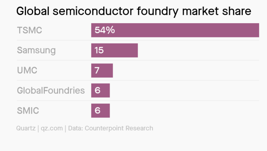
Largest Foundry Market Share
JDA #2 Customer – Major Semiconductor Foundry
High Capacity
Atomera announced that we entered into our second JDA, this time with a large semiconductor foundry who’s been working with us in phase 3 for a number of quarters.
This new JDA we announced today is pretty focused around one specific business. And if all goes well, they’ll be driving that specific one to get into production, and hopefully, will get adopted by other business units inside their company.
The purpose of which is to define exactly what steps will be taken with high priority and with a full set of resources to take MST-based products into production, if the results of our latest experiments meet their expectations.
Now, the first milestone requires us to get good results on some work that we’re doing together right now. But, the whole point of the JDA is to kind of grease the skids, that if we get good results on that next one — and we’re very confident.
That said, if we’re successful on this JDA, we believe the customer will move expeditiously towards commercialization because the all the legal and contract delays should be behind us.
But we do have a number of other areas that we have been talking with them about and has the real potential to expand beyond, into those once we’ve established success in this first area.
Foundry License – World Class Foundry
High Capacity
$75k license paid in q1 from North America
Licensee that started in February, and obviously, we’re going very hot and heavy with them.
Foundry partner very well known in the industry for bringing innovative technologies to market.
We started our engagement with them some time ago, so they are already a Phase 3 customer
Over the last year, they have used our MSTcad modeling software to unveil some compelling new uses of MST that may enhance some of their specialty processes.
Once that advantage was made clear to them through our modeling software, they immediately took steps to start running MST on device wafers.
Electrical results, which validate the modeling run by this new licensee, would be a breakthrough in performance that I think they would be extremely enthusiastic about taking into production.
Obviously, if our technology is adopted by a foundry and made a standard process, it opens the door to fabless design companies around the world designing chips that can be used in our process, and that’s quite exciting to us.
Any due diligence from this site is for entertainment only and not a solicitation to buy or sell Atomera stock. Any estimates are just examples of what is possible and should not be considered financial advise. I have not been compensated in any way and will never be compensated for my reports.